- 您现在的位置:买卖IC网 > Sheet目录3872 > PIC18F4450T-I/PT (Microchip Technology)IC PIC MCU FLASH 8KX16 44TQFP
142
XMEGA A [MANUAL]
8077I–AVR–11/2012
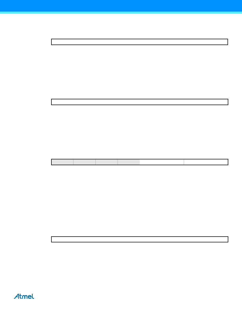
13.13.8 OUTTGL – Data Output Value Toggle register
Bit 7:0 – OUTTGL[7:0]: Port Data Output Value Toggle
This register can be used instead of a read-modify-write to toggle the output value of individual pins. Writing a one to a bit
will toggle the corresponding bit in the OUT register. Reading this register will return the value in the OUT register.
13.13.9 IN – Data Input Value register
Bit 7:0 – IN[7:0]: Data Input Value
This register shows the value present on the pins if the digital input driver is enabled. INn shows the value of pin n of the
port. The input is not sampled and cannot be read if the digital input buffers are disabled.
13.13.10 INTCTRL – Interrupt Control register
Bit 7:4 – Reserved
These bits are unused and reserved for future use. For compatibility with future devices, always write these bits to zero
when this register is written.
Bit 3:2/1:0 – INTnLVL[1:0]: Interrupt n Level
These bits enable port interrupt n and select the interrupt level as described in “Interrupts and Programmable Multilevel
13.13.11 INT0MASK – Interrupt 0 Mask register
Bit 7:0 – INT0MSK[7:0]: Interrupt 0 Mask bits
These bits are used to mask which pins can be used as sources for port interrupt 0. If INT0MASKn is written to one, pin
n is used as source for port interrupt 0.The input sense configuration for each pin is decided by the PINnCTRL registers.
Bit
765
4321
0
+0x07
OUTTGL[7:0]
Read/Write
R/W
Initial Value
000
0000
0
Bit
76543210
+0x08
IN[7:0]
Read/Write
RRRRRRRR
Initial Value
00000000
Bit
76543210
+0x09
–
INT1LVL[1:0]
INT0LVL[1:0]
Read/Write
RRRR
R/W
Initial Value
00000000
Bit
76543210
+0x0A
INT0MSK[7:0]
Read/Write
R/W
Initial Value
00000000
发布紧急采购,3分钟左右您将得到回复。
相关PDF资料
PIC18F4450T-I/ML
IC PIC MCU FLASH 8KX16 44QFN
PIC18F4321T-I/ML
IC PIC MCU FLASH 4KX16 44QFN
PIC18F4221T-I/ML
IC PIC MCU FLASH 2KX16 44QFN
PIC18F2321T-I/ML
IC PIC MCU FLASH 4KX16 28QFN
PIC18F2221T-I/SO
IC PIC MCU FLASH 2KX16 28SOIC
PIC16LF1939-I/MV
IC MCU 8BIT 28KB FLASH 40-UQFN
PIC24F16KL402-I/SP
IC MCU 16BIT 16KB FLASH 28-SPDIP
PIC18F24J11-I/SS
IC PIC MCU FLASH 16K 2V 28-SSOP
相关代理商/技术参数
PIC18F4455-BL
制造商:POWERLITE SYSTEMS 功能描述:PIC18F445 W/ BOOTLOADER FOR FLASHLAB 制造商:POWERLITE SYSTEMS 功能描述:PIC18F445 W/ BOOTLOADER, FOR FLASHLAB 制造商:POWERLITE SYSTEMS 功能描述:PIC18F445 W/ BOOTLOADER, FOR FLASHLAB; Silicon Manufacturer:Powerlite Systems; Core Architecture:PIC; Kit Contents:Board; Features:Bootloader Programming, RS232 Connector for Boot-Loading and Serial Comms ;RoHS Compliant: Yes
PIC18F4455-I/ML
功能描述:8位微控制器 -MCU 24kBF 2048RM FSUSB2 RoHS:否 制造商:Silicon Labs 核心:8051 处理器系列:C8051F39x 数据总线宽度:8 bit 最大时钟频率:50 MHz 程序存储器大小:16 KB 数据 RAM 大小:1 KB 片上 ADC:Yes 工作电源电压:1.8 V to 3.6 V 工作温度范围:- 40 C to + 105 C 封装 / 箱体:QFN-20 安装风格:SMD/SMT
PIC18F4455-I/P
功能描述:8位微控制器 -MCU 24kBF 2048RM FSUSB2 RoHS:否 制造商:Silicon Labs 核心:8051 处理器系列:C8051F39x 数据总线宽度:8 bit 最大时钟频率:50 MHz 程序存储器大小:16 KB 数据 RAM 大小:1 KB 片上 ADC:Yes 工作电源电压:1.8 V to 3.6 V 工作温度范围:- 40 C to + 105 C 封装 / 箱体:QFN-20 安装风格:SMD/SMT
PIC18F4455-I/PT
功能描述:8位微控制器 -MCU 24kBF 2048RM FSUSB2 RoHS:否 制造商:Silicon Labs 核心:8051 处理器系列:C8051F39x 数据总线宽度:8 bit 最大时钟频率:50 MHz 程序存储器大小:16 KB 数据 RAM 大小:1 KB 片上 ADC:Yes 工作电源电压:1.8 V to 3.6 V 工作温度范围:- 40 C to + 105 C 封装 / 箱体:QFN-20 安装风格:SMD/SMT
PIC18F4455T-I/ML
功能描述:8位微控制器 -MCU 24kBF 2048RM FSUSB2 RoHS:否 制造商:Silicon Labs 核心:8051 处理器系列:C8051F39x 数据总线宽度:8 bit 最大时钟频率:50 MHz 程序存储器大小:16 KB 数据 RAM 大小:1 KB 片上 ADC:Yes 工作电源电压:1.8 V to 3.6 V 工作温度范围:- 40 C to + 105 C 封装 / 箱体:QFN-20 安装风格:SMD/SMT
PIC18F4455T-I/PT
功能描述:8位微控制器 -MCU 24kBF 2048RM FSUSB2 RoHS:否 制造商:Silicon Labs 核心:8051 处理器系列:C8051F39x 数据总线宽度:8 bit 最大时钟频率:50 MHz 程序存储器大小:16 KB 数据 RAM 大小:1 KB 片上 ADC:Yes 工作电源电压:1.8 V to 3.6 V 工作温度范围:- 40 C to + 105 C 封装 / 箱体:QFN-20 安装风格:SMD/SMT
PIC18F4458-I/ML
功能描述:8位微控制器 -MCU 24KB Flash 2KB RAM RoHS:否 制造商:Silicon Labs 核心:8051 处理器系列:C8051F39x 数据总线宽度:8 bit 最大时钟频率:50 MHz 程序存储器大小:16 KB 数据 RAM 大小:1 KB 片上 ADC:Yes 工作电源电压:1.8 V to 3.6 V 工作温度范围:- 40 C to + 105 C 封装 / 箱体:QFN-20 安装风格:SMD/SMT
PIC18F4458-I/P
功能描述:8位微控制器 -MCU 24KB Flash 2KB RAM RoHS:否 制造商:Silicon Labs 核心:8051 处理器系列:C8051F39x 数据总线宽度:8 bit 最大时钟频率:50 MHz 程序存储器大小:16 KB 数据 RAM 大小:1 KB 片上 ADC:Yes 工作电源电压:1.8 V to 3.6 V 工作温度范围:- 40 C to + 105 C 封装 / 箱体:QFN-20 安装风格:SMD/SMT